PCB Milling/ru
|
English • العربية • български • català • čeština • Deutsch • Ελληνικά • español • فارسی • français • hrvatski • magyar • italiano • română • 日本語 • 한국어 • lietuvių • Nederlands • norsk • polski • português • русский • Türkçe • українська • 中文(中国大陆) • 中文(台灣) • עברית • azərbaycanca • |
Присоединяйтесь к переводу страницы!Пожалуйста, внесите свой вклад в перевод страницы
Release status: Concept
| Description | Collection of software helpful for milling PCBs and their application to RepRap
|
| License | unknown
|
| Author | |
| Contributors | |
| Based-on | |
| Categories | Electronics, PCB/Circuitry Making
|
| CAD Models | |
| External Link |
One obvious goal of making a RepRap replicatable is getting it to make it's own PCBs or other electronic circuitries.
PCB milling is one of the more promising ways of Automated Circuitry Making.
Recent firmwares understand a pretty standard flavour of GCode, opening the door to a lot of toolpaths already existing. This page describes a few promising ones.
Researchers have already milled out functional PCBs on the WolfStrap. Generation 7 Electronics boards are made this way regularly. Minimum isolation path width is about 0.4 mm. Not sufficient for typical SMD parts, but well working for 0.1" (2.54 mm) spaced IC pins. There's still room for improvement.
Contents
- 1 Software suites
- 2 Toolpaths found to work
- 3 Toolpaths found to work partially
- 4 Hardware Tools
- 5 Raw Material
- 6 Example Circuits
Software suites
(Should these be moved to Useful Software Packages ?)
While a gazillion of softwares for creating and manufacturing circuits and PCBs exists, it was surprisingly difficult to find a working combination. As RepRap is open source, we want also to use open source tools for designing RepRap stuff, of course.
All applications described claim to run on all major OSs: Linux, Windows, Mac OS X. Testing was done on Ubuntu 10.04, 64-bit version.
gEDA
gEDA is a software suite with schematic and PCB layout editor. While it looks a bit antiquated and made for experts only at the first glance, the major lack of this suite is an up to date tutorial. It appears to be the most reliable and powerful open source choice, easily on par with Eagle.
Installation on Linux
You want at least gschem, pcb and xgsch2pcb. On Debian/Ubuntu this can be installed as follows:
sudo apt-get install geda geda-utils geda-xgsch2pcb
The version currently coming with Debian/Ubuntu by default is pretty old. To get the latest features, which also includes a lot of improvements on the G-code exporter, you can either subscribe to Eugene's weekly builds:
sudo add-apt-repository ppa:mehanik/geda-unstable
sudo apt-get update     # fetch immediately
sudo apt-get upgrade
... or install from source:
sudo apt-get install build-essential autopoint bison intltool flex libgd2-xpm-dev
sudo apt-get install libdbus-1-dev libgtk2.0-dev
git clone git://git.gpleda.org/pcb.git pcb
cd pcb
./autogen.sh
./configure --disable-doc
make
src/pcbtest.sh  # use it
Installation on Windows
Traditionally, gEDA is a tool of the Unix world, still readily downloadable Windows builds exist:
- His note: this is mingw-based, not cygwin-based, and the installer exe only installs pcb at the moment (unzip the build-*.zip to get an "everything" install)
- Build with Installer by Institut für Quantenoptik, Hannover, Germany.
Installation on Mac OS X
Andreas Schweizer has just the right blog entry for installing gEDA on Mac OS X.
Quickstart
The secret of a good workflow with gEDA is starting with xgsch2pcb. You can use it by double-clicking a .gsch2pcb file.
Once you're in this tool, use it to open the other parts of the project. If you changed something in the schematic, save it and return to xgsch2pcb. Then use this tool's button to open the PCB. It will automatically offer to update the PCB. If you have used Eagle or KiCad before, that's pretty intuitive.
gerbv
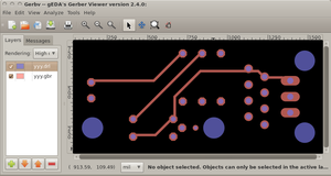
gerbv is part of the gEDA software suite and can view gerber files. This doesn't help directly, but is helpful in finding solutions and for troubleshooting.
Eagle
While Eagle is a proprietary and closed source tool; an almost full functional, free evaluation version exists. The only limitation of the free version is the maximum size of the resulting PCBs (100x80mm, 2 layers). Eagle is widely used among hobbyists and currently most RepRap designs are made with it, too.
Eagle is helpful for
- Schematic design.
- PCB design.
- Mill/Drill file creation (Gerber).
KiCad
KiCad is the rising star on the open source PCB creation sky. It's GPLv2 and in terms of features and user interface quite comparable to Eagle.
KiCad is helpful for
- Schematic design.
- PCB design.
- Mill/Drill file creation (Gerber).
- Creating offsets for isolation milling (HPGL).
Fritzing
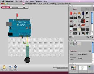
Fritzing is an open source schematic and PCB editor with a user interface for mere humans. As a highlight, you can pick and place electronic components just like you'd do this on a breadboard on your real desk. The schematic editor autoroutes connections similar to the PCB autorouter to tidy them up and all three parts - breadboard, schematic, PCB - are always kept in sync.
While this application is a very promising approach, it currently lacks a serious library. However, an Eagle to Fritzing converter is in the works, so this problem might be solved soon.
Fritzing is helpful for
- Schematic design.
- PCB design.
- Mill/Drill file creation (Gerber).
FlatCAM
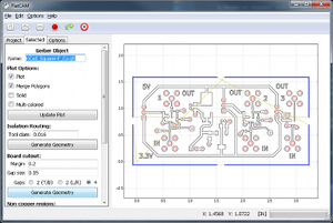
FlatCAM is yet another open-source "PCB to G-code" CAM application. It's written in Python and has been tested under Windows and Ubuntu.
Some of its core features are:
- Viewers/Handlers for Gerber, Excellon, G-Code.
- Create offset-type isolation routing geometry from Gerber.
- Create G-Code from arbitrary/other geometry, like board cutout.
- Helper for double sided PCBs.
Replath
Replath is RepRap's own effort to create a PCB manufacturing application. I'm not sure about it's status, as the last Wiki edit is from October 2008 and obviously the app's name got forgotten in the recent (September 2010) discussion about how to reprap PCBs.
Replath is helpful for
- Creating offsets for isolation milling.
- GCode isolation milling file creation.
- Sending the GCode file to the RepRap machine controller.
hp2xx
hp2xx is a very basic tool which can create GCode from HPGL. This is useful in conjunction with KiCad's export to HPGL outline feature.
hp2xx is helpful for
- GCode isolation milling file creation.
cam.py/cad.py
To quote from makeyourbot.org "cad.py is a CAM program that can be used to generate g-code tool paths for milling 2D and 3D objects. It operates on images instead of vector formats like Gerber, DXF, or SVG, so you'll have to export your board/object as a PNG image first. For larger objects without very fine features 200-300 dpi is fine, but for circuit boards I use 1000 dpi.
This page describes the general process."
Installation on Linux
Most modern Linux's come with Python already, but you might need special packages:
sudo apt-get install python-numpy python-scipy python-imaging-tk
Then run the script wherever you downloaded it by double-clicking.
Installation on Windows
In order to run cad.py on a Windows PC you need to install the following software:
- Python 2.6 (2.6 only!)
- Numerical Python (numpy)
- Scientific Library for Python (scipy)
- Python Imaging library (PIL)
How to use
You can download and run Neil Gershenfeld’s original cam.py or optimized cad.py by David Carr which in some cases this optimization reduces the milling path length by 50%, but is less tested. Lastly there is a cad.py that has been slightly modified so that it outputs '.gcode' instead of '.g' and has its preferences changed slightly.
In Eagle ...
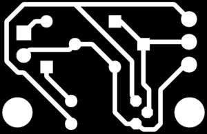
- Open your pcb and from the top menu select View->Display/Hide Layers and then deselect all but Top, pads and vias and then select ok.
- From the top menu again select File->Export->Image and choose monochrome and suitably high DPI. The larger the image file the lower the chance of traces overlapping, but requires a longer time to process. Images above 3000x3000pixels may result in a memory error. Then save as a .png.
In gEDA/PCB ...
- Open the layout and hide the layers you don't want. This is likely the silk and component layer, perhaps the outline layer.
- In the menu, choose File -> Export ..., then click "PNG". Select an appropriate DPI value, check "as-shown" and "monochrome". "only-visible" is also a good choice, but not neccessary. Leave all other boxes unchecked. Save the PNG to a convenient place.
In any case ...
- You might want to edit the image to get rid of unwanted contours, like those of drill holes.
- Load cad.py (or similar) and select "Input" and choose the .png image file created above.
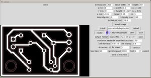
- Choose your settings such as x-width and y-width. Thses settings will determine the size of your PCB. By changing one and pressing enter, the other will be scaled to keep the right size ratio. Changing the max and min intensity is useful if your image is not completely black or white, but have a grey areas. The inches per unit changes the units for your pcb. By setting to 25.4 your x-width and y-width will be in mm. After changing any of the settings select 'render' to re-render the image.
- When ready to output your gcode select 'cam' and choose gcodes from the drop down menu.
- You may then adjust more settings such as 'minimum vector fit error (which alters how closely the tool path will match the image), tool diameter (in inches), tool overlap (a ratio) and feed rate (does not alter feed rate for reprap host, change the host settings).
- Once finished choosing your settings select 'contour' and wait for the processing to be done. Once completed, select save and the output .gcode (or .g) file will be in the same location as the image file.
- Load up the .gcode file with your desired host and print. This has only been tested with the Reprap host. You may want to undergo testing with a pen and plotting on paper before moving on to milling your first PCB.
Troubleshooting
If you run cad.py only to see a command prompt for a split second before returning to the desktop then it is most likely you have not installed all the required modules, software numbered 2 to 4 above. It is also possible that you have more than one version of python installed. Insure that you use python 2.6. Python 3 is quite different. Some people had success with the 32-bit version of python, only.
PCB-GCode
PCB-GCode is an add-on for Eagle, creating drill and isolation milling GCode files directly.
Installation on Linux, Mac OS X
PCB-GCode comes as a ZIP file. Unzip all the contents into one of your ULP folders, typically $HOME/.eagle/ulp. As the file permissions in this ZIP are found to be funny, PCB-GCode wants to write into it's installation folder (*sigh*), Eagle by default links $HOME/.eagle/ulp to /usr/share/eagle/ulp, you have to correct things a bit:
sudo chmod 777 $HOME/.eagle/ulp
cd $HOME
wget http://pcbgcode.org/file.php/download/12/93/pcb-gcode-3.5.2.11.zip
mkdir pcb-gcode
cd pcb-gcode
unzip ../pcb-gcode-3.5.2.11.zip
find . -type d -exec chmod 755 {} \;
find . -type f -exec chmod 644 {} \;
mv * $HOME/.eagle/ulp/
cd ..
rmdir pcb-gcode
Perhaps there's a simpler way, but this one worked for me.
pcb2gcode
pcb2gcode is a command-line program that calculates machine toolpaths from given PCB layouts. Despite it's name, it does NOT accept unix "pcb" files, but standard gerber RS274-X and Excellon files, and creates fully EMC2-compatible RS274-NGC files.
Installation
Find the latest sources at Sourceforge. Unpack them somewhere, change into it's directory and do:
sudo apt-get install build-essential libboost-all-dev libgtkmm-2.4-dev gerbv
./configure
make
# it's a single file application, no installation needed ...
./pcb2gcode --help
If you want to get the latest features download the latest development code from sourceforge (Code -> Download Snapshot), unpack them somewhere, change into it's directory and do:
sudo apt-get install build-essential libboost-all-dev libgtkmm-2.4-dev gerbv
./git-build.sh
sudo make install
man pcb2gcode
If you get a link error like "cannot find the library `/usr/lib/libgdk_pixbuf-2.0.la", you're hit by a temporary Ubuntu bug. Include the orbweaver PPA and upgrade packages to get it solved.
Note: pcb2gcode 1.0 used to not work on Ubuntu 10.04 64-bit. pcb2gcode 1.1.0 works fine on Ubuntu 10.10 32-bit and 64-bit.
Quickstart
User:Lanthan on 20101024 comments: I got pcb2gcode to compile and it appears to work adequately on Ubuntu 10.04 Lucid 10.04 (RTAI). The most interesting option (IMHO) is to generate a trace isolation voronoi map. I am testing it with Generation 7 Electronics.
Here is my current millproject file (as of 20101113) :
# this is an example config file for pcb2gcode.
# place this in the same directory as your gerber files to save typing

# You may want to uncomment and change those in local project files
#front=Gen7Board.front.gbr
back=Gen7Board.back.gbr
drill=Gen7Board.plated-drill.cnc
#outline=contour.back.gbr
#verbose

# parameters for isolation routing / engraving / etching
zwork=-0.008
zsafe=0.8
zchange=1.0
mill-feed=6
mill-speed=30000

# parameters for cutting out boards
cutter-diameter=0.059055118
zcut=-0.08
cut-feed=3
cut-speed=20000
cut-infeed=1

# drilling parameters
zdrill=-0.08
drill-feed=3
drill-speed=20000

#offset=0.006
# generate voronoi regions
offset=1.0
dpi=1000
#max-deviation=0
A few notes:
- The coordinate's origin is the origin of the whole Gerber file, the outline drawn in gEDA/pcb is ignored. This is a contribution to the fact pcb2gcode isn't integrated into gEDA/pcb. Coordinates are flipped from top to bottom, so expect an offset of
X = X coordinate of the leftmost point of the outline

Y = total vertical layout size - Y coordinate of the lowest point of the outline
You can use --zero-start to set the origin at (0,0)
- To compensate for the above and make pcb2gcode output compatible with gEDA/pcb (with patches applied) G-Code export, offset the machine by the above X and Y values into the negative.
- To get voronoi mill paths, use a very high offset. pcb2gcode will complain about it's failure, but it's "best effort approach" will do the right thing.
-
The generated G-Code files are huuuuge, a real stress test for the FiveD G-Code interpreter. gEDA/pcb's built-in G-Code generator does a lot better, but can't create center/voronoi paths. Using the --dpi option can make mill files smaller, at the cost of accuracy.Newer versions of the software accepts the --optimise command line option that greatly reduces the output G-Code (~95%) without any significant loss in precision.
cynbes-gcoder
Cynbe's GCoder is an early version of pcb2gcode which was found to actually work.
Installation
sudo apt-get install gerbv
wget http://muq.org/~cynbe/gcoder/cynbes-gcoder-2008-12-21-04.49.09.tbz
tar -xvjf cynbes-gcoder-2008-12-21-04.49.09.tbz
cd cynbes-gcoder
make
./cynbes-gcoder --help
Quickstart
Do it in cynbes-gcoder's directory, it comes right with sample gerber files:
./cynbes-gcoder -v --cu=0.0007 --bit=60 --drill=qdrill.cnc qtop.gbr
The resulting files have the suffix .ngc.
GCAM
GCAM Is a GUI-based tool claiming to handle Gerber files, and of course outputting GCode files.
Installation
For more detailed instructions, see [1].
Everybody except Windows and 32-bit Ubuntu users has to compile from source:
# probably apt-get install something, but here it compiled without any
sudo apt-get install build-essential libgtkglext1-dev
wget http://gcam.js.cx/files/gcam-2010.07.27.tar.gz
tar -xvzf gcam*
cd gcam*
./configure --prefix=${PWD}/installation # install locally for now
make && make install
./installation/bin/gcam # test it!
Visolate
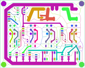
There's an application which does something quite interesting: instead of framing each track, it calculates the median line/curve between each pair of tracks and mills these. This minimises milling time and maximises track width. The latter is important for high-current tracks.
You can find Visolate 3 and later on Github. There are also downloads of Visolate JAR files, which can be used as-is, without installation.
Simple Usage
To use Visolate, run it in a terminal with the Java engine:
java -jar visolate-3.0.jar
If this results in error gibberish, see installation instructions below.
The most simple use case is to load a Gerber file at the top of the window, then clicking "Fix Topology" and "Make Toolpaths", then saving the G-code file. For all the options in between, move your mouse over all the buttons and fields. Tooltips appear which shall be helpful.
Accuracy of the G-code is adjusted by adjusting the DPI value of the display. The finer the accuracy, the more lines of G-code you get. Typical values are between 100 and 5000 dpi.
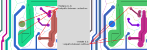
Differences between Visolate 2 and Visolate 3
- Toolspaths now respect the thickness of elements. Earlier, only the centers of tracks/pads were taken for calculation, now the entire perimeters are. See (and click on the) picture to the right.
- Path junctions are now kept accurately.
- Much faster path optimisation. Now fast enough to allow removal of the secondary progress bar.
Installation on Linux
Visolate requires some non-standard libraries and handling non-standard libraries is an area where Java not exactly shines. This one is apparently the right approach for running Visolate 3 on Ubuntu 12.04:
sudo apt-get install --no-install-recommends openjdk-6-jre
sudo apt-get install --no-install-recommends libjava3d-java libjava3d-jni libvecmath-java
java -jar visolate-3.0.1.jar
Earlier, this one used to work on Ubuntu with a few tweaks:
sudo apt-get install --no-install-recommends openjdk-6-jre
sudo apt-get install --no-install-recommends libjava3d-java libjava3d-jni libvecmath-java
sudo update-java-alternatives -s java-6-openjdk
sudo ln -s /usr/share/java/j3dcore.jar /usr/lib/jvm/java-6-openjdk/jre/lib/ext
sudo ln -s /usr/share/java/j3dutils.jar /usr/lib/jvm/java-6-openjdk/jre/lib/ext
sudo ln -s /usr/share/java/vecmath.jar /usr/lib/jvm/java-6-openjdk/jre/lib/ext
java -jar visolate-2.1.6.jar  # or visolate-3.0.jar
Thanks a ton to User:Xsainnz for helping to find the latter out.
Oh, and make sure the fglrx package (nVidia graphics drivers) is not installed on computers with Intel graphics. EMC2 pulls that in as a dependency.
Installation on Windows and other platforms
On other systems Visolate requires at least the following dependencies to be installed:
1) java Develoment Kit for example Java Standard Edition Development Kit available here.
2) java3D package (32-bit?), binaries can be downloaded from here
For windows run the *.jar file. For this purpose, in the folder where the visolate's jar file is located make a new text file containing only one line "java -jar [filename].jar", without quotes, and with the correct *.jar name, for example "java -jar visolate-3.1.1.jar". Rename the text file with .bat extension, e.g. "visolate.bat". Double click the bat file to run visolate, this will provide a parallel "terminal" window which lists program's output, useful for debug and information purposes. There are other ways to run the jar file, this is just one way.
Usage details
Visolate is a bit unintuitive in it's usage, still it can create excellent results.
A few additional notes:
- Most text fields and checkboxes have tooltips, so hoover over them to read what their purpose is and to find out how Visolate works.
- Visolate loads Gerber files, but Gerber polygons are not (yet) supported. You get a message containing "TBD polygon mode" if you run Visolate from the command line and attempt to load such a file anyways.
- You can "fix" a Gerber by opening it with a text editor and removing all lines containing "G36", all lines containing "G37" and all the lines in between such a pair. You loose some geometry, though, so the usefulness of this hint varies. For samples of G36/G37 pairs, and the Gerber file format in general, see the Gerber RS274X format description.
- gEDA/PCB uses such unsupported polygons to draw non-round pins. For Voronoi mill paths, round pins are just as fine, so open the .pcb file and remove all occurences of "octagon" and "square" in pin definitions. Then, reload the layout in gEDA/PCB and export a Gerber again.
- In the Visolate GUI, only the sections "G-Code" and "Processing" affect the output. Exception is the "Geometry" -> "flip" checkbox.
- Use "left upper coordinates" to adjust the G-Code's origin.
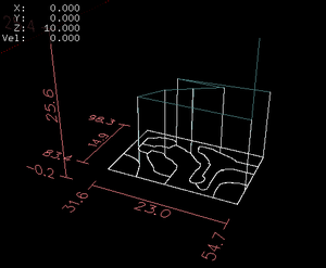
- Review the produced G-code in a G-code viewer until you gain some experience, especially on how different DPI setting influence the granularity of this G-code.
Additional web pages are an older project page and a Sourceforge repository.
EMC2
Without doubt, EMC is made for dedicating a generic PC into a machine controller. This is pretty intrusive, for example it installs a realtime kernel module. The good news is, EMC2 also has a simulation mode installation, which is apparently much less intrusive.
Installation
About any set of installation instructions for EMC2 talks about using their Ubuntu LiveCD and misses the simulation variant, but there's a pretty simple way to set this up on a generic Ubuntu:
- Go to EMC2's package directory directly, plunge into the directory for your variant of Ubuntu (32-bit or 64-bit) and look for a file named starting with "emc2-sim_2.4" and ending with ".deb". Download this.
- Install this package by double-clicking it (and a few additional, obvious steps).
- In your applications menu you'll find now CNC -> EMC2. Start this.
- EMC2 will ask you for a machine configuration. Choose "sim -> mini", this was one of the few configurations I found to work.
This won't give anything to create those files, but a nice facility for simulating GCode files created with other applications.
If you want to build from source, or the previous link just won't do the trick, you can follow the instruction here: LinuxCNC wiki:Build A Simulator Manually. It works for almost any version of Ubuntu. Tested on 64bit Ubuntu 12.04 Precise.
- Note: In recent Ubuntus, there's no need to sudo apt-get purge tcl8.4-dev tk8.4-dev, the sim runs perfect anyways.
Incompatibilities
The emc2 package has the fglrx package as a dependency, which is incompatible with Intel graphics drivers. You can install EMC2 on a computer with Intel graphics and it will work, but all applications using OpenGL (e.g. RepRap Host) will stop working until you remove the fglrx package again.
CNC Gcode Controller
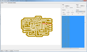
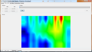
Is a host software optimised for milling and autoleveling it also Optimise you Gcode! See CNCGcodeController
Toolpaths found to work
Toolpaths found here give a full solution from the PCB editor to creation of RepRap firmware compatible GCode.
For sending GCode to the machine controller, one can use RepRap Host software or any terminal emulation software capable of connection to a real serial device in conjunction with a firmware capable of doing flow control, e.g. Teacup Firmware.
Eagle -> PCB-GCode -> GCode
Once it's installed, PCB-GCode works just nicely. Type
run pcb-gcode-setup
in Eagle's command line, hit Enter, modify settings to what you need, then click "Accept and make my board". If any question dialogs appear, you can answer them always with Yes. A GCode preview will appear, type 'x' or 'q' to leave it. After that, a bunch of GCode files show up in the project's directory, which are (almost) ready to be sent to the RepRap machine.
Hint: Use CNCGcodeController as Host Software its optimised for this setting!
Settings
That's already well documented, see 10bull's web page, Christoph Selig's Blog (german, but with pictures) and of course PCB-GCode's own documentation, which is part of the code distribution and typically ends up in $HOME/.eagle/ulp/docs/readme.html.
Highlights
- Can follow an isolation path multiple times with raising offset. This is needed when using engraving tips as tools.
- Can mill arbitrary geometries. Just put lines (wires) or arcs on layer 46 "Milling" and the appropriate GCode will appear.
- Mills any text put on layer 46 "Milling" with a single milling vector, so text is actually readable.
- Strategy for manual tool change included:
- The tool head will move to the tool change position (typically up in the air).
- Change the tool and fix it in a position too short for milling.
- Continue to run the GCode, it will stop at X=0, Y=0, Z=0.
- Loosen the tool a bit and let it drop onto the PCB's surface.
- Tighten the tool holder again and your tool should be right at the correct length.
Missing Features
- Ability to mill larger holes with the milling tool. PCB-GCode asks for an appropriate drill for each of the used hole diameters. This eventually requires a lot of tool changes and a well sorted tool rack.
- Ability to replace curved movements (G02/G03) with a set of straight movements (G01).
- Ability to mill circles, rectangles or polygons. A workaround is to replace them with lines and arcs.
gEDA/pcb -> G-code
Recent versions of gEDA (August 2010 or later) come with an G-code exporter. On how to install a current version of pcb, see above.
Here's a File:GEDA-pcb-milling-patchset.zip you can apply before building pcb from source. Unpack the set, then do
git am < xxx.patch
for each of the patches, starting with 0001-xxx.patch. Another source for the patches is gEDA's patch tracker.
Highlights
- With the patchset, the exported G-code is FiveD_on_Arduino compatible.
- No G02/G03 circled movements. For some RepRap controllers, this is a plus.
- With the patchset, pre-drilling of bores with the engraving bit. Avoids inaccurate bore positions and snapped drills.
- With the patchset, drill-milling (drilling all bores >= mill diameter by milling a circle), so fewer tool changes.
Missing Features
- No line numbers and no checksum calculation, so no compatibility with official FiveD.
- No Voronoi mode.
gEDA/pcb -> gerber and excellon -> pcb2gcode -> G-code -> EMC2/Axis -> tabletop CNC
This does not need patched gEDA and most probably works also with gerber & excellon files generated by Eagle. Tested with Ubuntu 10.04 32 bits
Highlights
- put all configuration parameters in a "millproject" text file in the same directory as your gerber files: saves a bunch of typing!
- Voronoi regions if wanted
- use a "vendor mapping" file with gEDA/pcb to significantly reduce the number of drill sizes it will be asking for
- Have a look at the gcode of the drilling files (the interactive 3D display of Axis helps a lot!) and further check drill sizes if needed.
- doesn't insist on mirroring the drill and the pcb-back files: good!
- I am using a 60 degrees v-bit with 0.2 mm flat tip. Wonderful results, didn't need any de-burring.
- Still too deep at Z=-0.1 mm wil be testing milling at z = -0.03 mm
- Beware of the tiny white itchy-scratchy powder if you're milling glass fiber boards.
Limits
- Voronoi regions generated code un-optimized but works great anyway and tests your machine's repeatability ;-)
- All imperial measures endeavour, if you live in mm world you will have to translate your sizes to mils. EMC/Axis has no problem with 'em but still reports coordinates in the original machine units (mm)
Toolpaths found to work partially
Toolpaths which mostly work, but lack some needed features. One example would be generation of valid isolation mill paths, but no GCode for drilling.
Hardware Tools
A few words about useful hardware tools ...
Spindle
Obviously, you need a spindle motor. The faster this spindle is, the better. You can get away with 5.000 RPM and a lot of patience. 10.000 RPM are better, as this cuts manufacturing time by almost 50%. Professional machines have 100.000 RPM or more.
Also, the spindle's bearings should be free of play. As we're going to use mills in the sub-millimetre range, a play of 0.1 mm is already too much. Some motors reduce their play as they warm up.
Power/wattage of the motor is no point to worry about, though. The power needed to drive a 0.8 mm mill or drill is probably less than 10 Watts.
For more insight and some low cost spindle variants, see Milling and Drilling Head.
Milling tools
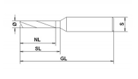
When it gets to milling tools, there is more than one choice. One has success with end mills, others swear on engraving tips of various sizes. The only thing all people agree about is: the non-sharp end has to fit into the spindle's chuck.
End Mills
The advantage of end mills is, you can achieve higher feed rates. When driving horizontally, they do all cutting at the outer perimeter.
The disadvantage is, they are of constant thickness along the rotation axis, making them weak. Diameters down to 0.3 mm exist, but you break them by just looking sharply. Thicker diameters like 1.0 mm are already too thick to isolate between the pin pads of ICs, much less you can draw traces between such pads.
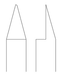
Engraving Tips
These don't allow feed rates as high as end mills, but due to their angle, they are relative stiff while still allowing isolation cuts down to 0.2 mm.
Opinions are different about which tool angle is the best. Some use 90 deg tools, others report best results with 60 degs, even others use exclusively 10 deg tips.
Common to this type of tools is, the isolation path gets wider the deeper you plunge the tool into the material. Accordingly, the PCB raw material has to be very flat and well leveled to the machine. Try to allow no more than 0.1 mm.
The additional widening of the isolation gap is
2 * penetration depth * tangens ( tool tip angle / 2 )
That results in 17% of the penetration depth for a 10 deg tip, 54% for 30 deg, 115% for the 60 deg version and no less than 200% for a 90 deg tool tip angle. 0.1 mm additional penetration depth means a 0.2 mm wider isolation gap in the latter case.
Judging by reports found on the net, sharper tips have a stronger tendency for burr, so - like always in life - the best angle is a compromise.
Raw Material
Raw material is usually a copper plated sheet of some isolating material and some choices exist. For the german speakers among us, there's a good comparison sheet on the net.
FR-2
FR-2 (e.g. Pertinax) is typically of dark yellow to brownish colour. Often used for cheap electronic devices, it's also the easiest one to machine. In other words, it takes quite some time until your tool becomes dull.
FR-4
FR-4 (glass fiber reinforced epoxy) is a lot stronger and is available as two-sided sheet as well. However, due to the glass fibers, even carbide tools wont last forever. Or, like some core team member said: "It eats bits like nothing".
Other raw materials
Whatever you can mill, will work, of course.
Example Circuits
Examples made on a WolfStrap
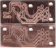
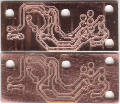
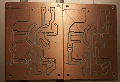
This shows a PCB for an Opto Endstop 2.1, modified to be single-sided: path widths 0.5 mm, Restring 40% (about 0.32 mm). GCode generator was pcbgcode on Eagle, milling depth set to 0.2 mm, mill path width set to 0.36 mm. Milling tool for the paths was a 30 deg engraving tip, a 0.7 mm drill for all small holes and an 1.0 mm end mill for the bigger holes and for the outer cut.
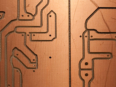
Both PCBs are actually the same, photoshop'd together. The scanner used for making the photos puts more emphasis on the scratches than are visible in natural. The upper view shows the PCB as it came off the machine, the lower one after deburring on a grind stone (typically used for sharpening knifes). The mill paths width actually achieved is about 0.41 mm. Notably are inaccuracies due to the play of the threaded rod driven machine (see bone-shaped path to the lower left) and the tendency for a bridging chip where narrow mill paths are close enough to meet in a sharp angle (see near top center).
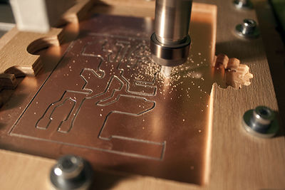
Examples made on a tabletop cnc router
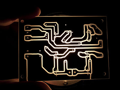
60 degrees cheap v-bit, 0.1 mm depth (still too much), no deburring needed at all.
Examples on the Net
- Opto Endstop made by Gavilan.
- Fabio: Arduino compatible microcontroller board, specifically designed to be easy to make a on a milling machine -- single-sided, relative large trace/space, etc.
- Hydra doing PCB milling by Clayton.
- Adventures with Atmel AVRs and CNC PCB engraving by Alan Garfield.
- TINYPOV Milling Challenge by Gatonero.
- First PCB milling success gives a few good hints on how to avoid burr.
- BuildYourCNC.com : "Printed Circuit Board Isolation Routing"[2]: using EAGLE, PCB-Gcode, etc.
- Where do the copper flakes come from: notes on PCB milling on repraps
