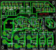
RDB G 001
Generic pages: | Introduction | Naming convention | TS Interfaces | Feature Interfaces | Steppers Interfaces | RDB_calibrations | RDB_DIY_tips |
Specific pages: | RDB_TS_G_001 |
Release status: experimental
| Description | Generic development board extension for 3D printing
|
| License | |
| Author | |
| Contributors | |
| Based-on | |
| Categories | |
| CAD Models | |
| External Link |
Contents
Features Overview
This board is meant to take GPIO wires from the development board and provides the basic functions, that is switches (for hotends heating), thermistors (for temperature reading) and also endstops headers in two different configurations. Board features:
-Voltage regulators: 2 (adjustable)
-Headers: 3+3 endstops
-Thermistors: 5
-Switches: 4xMosfets(Vdc) & 1xTriac(Vac)
-Pcb size: ~ 10x9 cm
-optimized for DIY: single sided, clearance 0.508mm, min track width 1.5mm, format and traces "bulky" enough so board could be made with any technique.
What this is not
- This board is NOT a shield, connections require physical wiring between this and development board.
- This does not contain any mcu.
- This does not contain stepper drivers or anything to do with them. The logic here is that steppers are to be driven separately with step/dir/en lines taken directly from GPIO of development board. Hence are of no concern for this board.
- For other more "integrated" electronics see List_of_electronics
Power input
- simple reverse polarity protection with high current diode and fuse
- transient supressor
- max input voltage depends on the regulators used
Voltage regulators
- two adjustable voltage regulators, in paralel configuration
- multiturn adjustment pots
- voltage regulators are 3 terminal type, TO-220 package, e.g.: LM317 LM1086, and similar pinout compatibility (TO220 with middle pin Vout)
- first regulator purposed for development board supply and mosfet driving
- second regulator is logic voltage of the board
Thermistors
- ADC pins come from development board, are broken into 5 headers to be further connected to thermistors physical location.
Endstops
- 3 endstop headers with hardware pullups and protection diodes
These endstops need to sink the current for normal operation and disconnect the line when triggered.
- 3 endstop headers with hardware pullups and optoisolators
These need to provide current to the optos internal led to keep it lit up for normal operation, and disconnect when triggered. The headers with optoisolators are meant to be somewhat universal and support almost any configuration. They have their own separate power connector (v+ and gnd). Visual indicator leds are in same loop with isolators internal leds, so these lit up always in normal operation. Only when endstop is triggered the visual indicators also turn off. With default values these should work with traditional reprap 5v optoendstops, directly, without other components (no optos boards). For alternate configurations and other sensors the current limiting resistors need to be adjusted according to voltage used and current required.
Switches
All switching components are to-220 package, 3 terminal, with heatsink space for standard to220 radiators and are placed in line for alternative common backplate type sink with 2 points fixture. Mosfets switches use their own connection paths and are not connected to the board's input ground.
Low side MOSFET Switches (vdc)
- 2 mosfets with fuse sockets, presumed for high current (bed and hotend)
- 2 mosfets without fuses
Truth table: feature active when high
| logic level | Behavior |
|---|---|
| high | conducting |
| low | non-conducting |
The fets leds are kind of counter-intuitive, because are tied in paralel to the mosfet. So leds are off when fet is conducting. If there is a load connected, the leds switch on when and mosfet is not conducting. The fets have some optional micro-snubbers, mostly because needed to leave space for standard to-220 radiator "hat" type. Normally snubbers need to be tweaked and then tested in order to make them effective, but on the other hand the default values should provide "something" which cant hurt, to say so.
Triac Switch (vac)
- 1 (optional) zero-crossing optocoupler commanding a triac for on-off control of one Vac line
Triac is optional, for ac switching. It can be used to switch some spindle motor, or if the bed is supplied with ac. This is on-off control only (not proportional, does not change the firing angle). Mains voltages are dangerous, so use this with care and wisdom. Ensure minimal distances and good isolation of the board where the mains circuit is located. Ensure no shorts can possibly occur anywhere: shorting 230vac to 5vdc isnt pretty. Be warned.
Truth table: connected to transistor's base / fet gate, feature active high
| logic level | Behavior |
|---|---|
| high | conducting |
| low | non-conducting |
Triac by default uses an zero crossing optocoupler, for better switching, so its max switching speed depends on the AC frequency. Triac should be snubberless type (not needing snubber). Unlike fets leds, triac led is normal, e.g. led is on when triac is on and vice-versa.
The logic level command signal can be tied in two ways in the 2 wire connector. If connected through the to92 transistor, this will conduct the line to ground, so triac will be active when the the logic signal is high. If connected to the drive line directly, it needs to sink the current into the uC GPIO itself, so the triac will be active when the logic signal is low. So, second mode of operation is possible, but not wise, and is also inverted of the first (feature enabled when low and disabled when high).
Source files
Schematic: download as PDF file
Kicad source files: download Kicad files - version 001alpha - last updated: April 2013
