Advances in plasmonic light trapping in thin-film solar photovoltaic devices

|
By Michigan Tech's Open Sustainability Technology Lab.
Wanted: Students to make a distributed future with solar-powered open-source RepRap 3-D printing and recyclebot recycling. |

|
Source
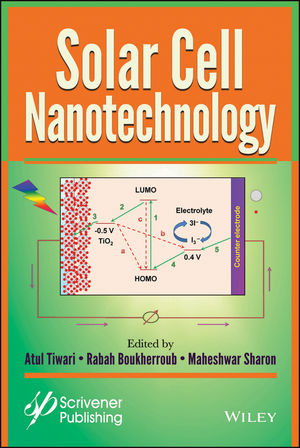
J. Gwamuri, D. Ö. Güney and J. M. Pearce, "Advances in Plasmonic Light Trapping in Thin-Film Solar Photovoltaic Devices", in Solar Cell Nanotechnology, Atul Tiwari (Editor), Rabah Boukherroub (Editor), Maheshwar Sharon (Editor), Wiley, ISBN: 978-1-118-68625-6 Preorder
Abstract
This chapter reviews the recent promising advances in the use of plasmonic nanostructures forming metamaterials to improve absorption of light in thin-film solar photovoltaic (PV) devices. Sophisticated light management in thin-film PV has become increasingly important to ensure absorption of the entire solar spectrum while reducing semiconductor absorber layer thicknesses, which reduces deposition time, material use, embodied energy and greenhouse gas emissions, and economic costs. Metal nanostructures have a strong interaction with light, which enables unprecedented control over the propagation and the trapping of light in the absorber layer of thin-film PV. The literature is reviewed for both theoretical and experimental work on multiple nanoscale geometries of plasmonic absorbers and PV materials. Finally, the use of nanostructures to improve light trapping in PV is outlined to guide development in the future.
See also
- Plasmonic Perfect Meta-Absobers for a-Si PV Devices
- Multi-resonant silver nano-disk patterned thin film hydrogenated amorphous silicon solar cells for Staebler-Wronski effect compensation
- Controlling optical absorption in metamaterial absorbers for plasmonic solar cells
- Limitations of ultra-thin transparent conducting oxides for integration into plasmonic-enhanced thin-film solar photovoltaic devices
- Optical modelling of thin film microstructures literature review
- Multi-resonant silver nano-disk patterned thin film hydrogenated amorphous silicon solar cells for Staebler-Wronski effect compensation
- Effect of ambient combinations of argon, oxygen, and hydrogen on the properties of DC magnetron sputtered indium tin oxide films
- Influence of Oxygen Concentration on the Performance of Ultra-Thin RF Magnetron Sputter Deposited Indium Tin Oxide Films as a Top Electrode for Photovoltaic Devices
- A new method of preparing highly conductive ultra-thin indium tin oxide for plasmonic-enhanced thin film solar photovoltaic devices
- Plasmonic enhancement of amorphous silicon solar photovoltaic cells with hexagonal silver arrays made with nanosphere lithography
- Enhancement of hydrogenated amorphous silicon solar cells with front-surface hexagonal plasmonic arrays from nanoscale lithography
- Fabricating Ordered 2-D Nano-Structured Arrays Using Nanosphere Lithography
- Ambiance-dependent Agglomeration and Surface-enhanced Raman Spectroscopy Response of Self-assembled Silver Nano-particles for Plasmonic Photovoltaic Devices
- Micromorphology analysis of sputtered indium tin oxide fabricated with variable ambient combinations
- Optimal Design of Thin-film Plasmonic Solar Cells using Differential Evolution Optimization Algorithms
- MACE nano-texture process applicable for both single- and multi-crystalline diamond-wire sawn Si solar cells
- Scalable honeycomb top contact to increase the light absorption and reduce the series resistance of thin film solar cells
