DarwinPowerAndCommunicationsCard
The Communications and Power Distribution Board
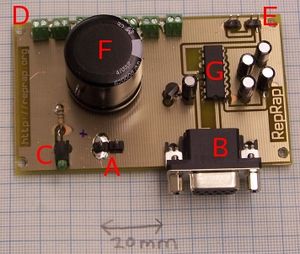
It consists of a power input connector (A) that is the 12v supply for the whole RepRap machine, and an RS232 connector (B) that is the communications link to the computer controlling the machine. (C) is a power-on indicator LED. There is a row of seven power output connectors at (D); these are wired into the other circuit boards in the RepRap machine to power them (only five are used for the Darwin design; the other two are spare). The RS232 signals are converted to and from 5v TTL levels by the chip (G) and its associated capacitors. The data from (G) to and from RepRap's communications ring is sent and received by the connectors at (E). (F) is a large smoothing capacitor to keep the 12v supply clean.
This is based on the older, stripboard comms controller designed by Simon.
All the KiCad files for this design are at svn/reprap/electronics/Comms_and_power_distribution
Build Board
Printed Circuit Board
Insert Real Image of Printed Board
Note that it has large ground and 12v planes on the two sides of the board. This both saves etching chemicals and also handles the current needed by all the other RepRap boards.
Build PCB
Here is a [[pdf of the power and comms board circuit ready for printing.|thumb]]
Use that and follow the instructions on how to make your own PCBs.
Buy PCB
- If you'd like to be added as a supplier, please contact the RepRap team.
Build Process
You'll need a soldering toolkit to do most of this.
Consumables
| Item | Name | Quantity | What Is It? | Mouser Part# |
| PCB | Comms Board PCB | 1 | a printed circuit board that holds the components | n/a |
| C1 | 100uF electrolytic 16v | 1 | an ElectrolyticCapacitor | 140-HTRL16V100-RC |
| C2-C5 | 1uF electrolytic 50v | 4 | an ElectrolyticCapacitor | 140-XRL50V1.0-RC |
| C6 | 4700uF electrolytic 30v | 1 | an ElectrolyticCapacitor | 140-XRL50V4700-RC |
| D1 | LED | 1 | a LightEmittingDiode | 859-LTL-4234 |
| J1 | 9-pin female PCB-mounting D connector | 1 | a female 9-pin serial connector | KF22X-E9S-NJ |
| P1 | 2 pin high current connector 5.08 mm | 1 | a power connector | 571-14376711 |
| P2,P3 | 2 pin connector 2.54 mm | 2 | signal connectors for token ring | 571-103239-2 ? |
| P4-P10 | 2 pin screw connector 2.54 mm | 7 | power connectors for other boards | ??? |
| R1 | 560 ohm | 1 | a resistor | 660-CF1/2C561J |
| U1 | 78L05 | 1 | a 5V voltage regulator | 512-LM78L05ACZX |
| U2 | MAX232 | 1 | a chip to help communicate with the serial port | 595-MAX232D |
Note: If U2 is replaced with a MAX202, C2-C5 can be replaced with 0.1uF ceramic capacitors.
Fabrication
You may want to look over our electronics fabrication guide before you start soldering.
Solder in all the components except U2 and its four associated capacitors (C2...C5).
If you etch your own PCB it will not be through-plated. This can make it hard to solder those components with flat bases that need to be soldered to the component side of the PCB. A good way to solve this is to tin round the hole where the component's leg is to go, then to tin the leg too. Now put the leg through the hole and touch the soldering iron onto the end of it sticking out of the bottom of the PCB. This melts the tinning and allows the component to be soldered in place. Alternatively, if the tinning on the PCB extends a bit beyond the periphery of the component, you can touch the soldering iron down there on the component side.
9-pin PCB D connectors come with a variety of ways of attaching them to the PCB in addition to the actual active pins. There are two pads on the PCB to drill out and mount these through, though different designs put the mountings in different places. If your connector coincides with those holes, all well and good. But if it doesn't it may be simplest just to cut/saw-off the mountings and rely on the pins to hold the connector in place. This should be quite strong enough. Under no circumstances use a mounting method that shorts the top (+) and bottom (-) layers of the PCB - these are opposite poles of the 12v supply...
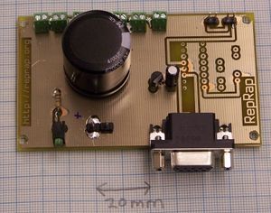
This first construction step should give a board looking like this:
Attach 12v power to the power connector (+ on the left in the photo, ground on the right) and check that the LED lights up. If it doesn't, you've made a mistake. Next put a voltmeter on the tracks that will connect to pins 15 and 16 of U2. This should measure 5v from the voltage regulator U1. If it doesn't, you've made a(nother) mistake...
Disconnect the power. Solder in U1 and C2...C5. Take particular care with the capacitors to get the polarity right - check with the circuit diagram which pins on U1 the positive and negative ends go to, and folow the tracks on the PCB. Then check it all again before you next apply power.
Congratulations! You have finished your first RepRap circuit.
Buy Board
Technical Stuff
Circuit and Description
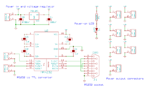
P1 is the main 12v power input connector - make this chunky. It can either be a screw connector, or - more elegantly - a plug. The 12v supply is taken straight through (via a big smoothing capacitor) to P4...P10. These are the power distribution lines to the rest of the RepRap PCBs. There are two spare - you only need five for the Darwin design.
DB9 is a female PCB-mounting 9-pin RS232 socket. Serial data from your computer comes in here, is converted to TTL voltage levels by U2, and is fed out to the rest of the RepRap PCBs via P2 and P3. Remember that RepRap communicates using a token ring, so only two connectors are needed for data. U2 gets the 5v power it needs from U1.
Finally there is an indicator LED so you can remember when you've left your RepRap switched on...
- If you'd like to be added to the suppliers, please contact the RepRap team.
-- Main.AdrianBowyer - 01 Nov 2006


