Howto PCB from Eagle
Contents
Intro
3D printer can be a very helpful tool when creating PCB (Printed Circuit Board). Here I try to summarize some practical experience.
Another approach using more complex toolchain is here (1)
Eagle Output in HPGL
Eagle is a very widely used tool for PCB creation. It has multiple formats for board layout output available under "CAM processor". Out of these the HPGL (HP graphic language) is quite well readable and its structure somewhat resembles G-code used in 3D printers.
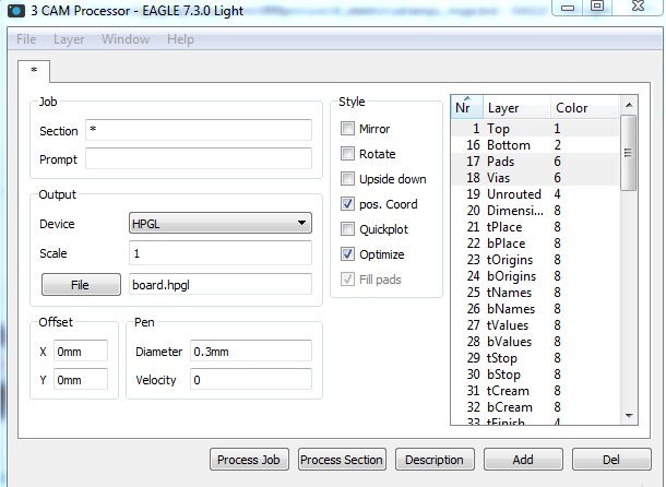
This is an Eagle dialog screenshot showing export to HPGL. Important settings: Device: HPGL, Scale: 1, File: your filename, Diameter: 0.3 (should correspond with diameter of your drawing pen. Make also sure that layers Top, Pads and Vias has been selected. Use button "Process Job" to generate output file.
Convert HPGL to G code
HPGL structure is not too distant from G code, moreover eagle apparently relies just on a limited subset of commands that are easily translatable to G Code.
- PU - Pen Up - corresponds with G1 Zxx
- PD - Pen Down - G1 Z0
- PA x,y - Plot Absolute - G1 Xxx Yyy
- Another important fact is that HPGL doesn't use mm but plotter units in PA command. There is 40.2 plotter units per mm .
For conversion, there's a web app available at: http://hpgl2gcode-4646.rhcloud.com
Or you can find a very basic python script here: http://github.com/gogela/hpgl2gcode
Make sure that resulting G code raises Z axis above 0 prior any moves, so you prevent plotting a random line over your PCB.
Fastening PCB sheet
It is a good practice to remove any traces of fat from the PCB before plotting (isopropyl works fine). Paper clips usually work fine to keep the board in place.
Pen
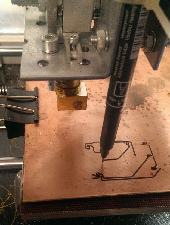
The PCB creation was successfully tested with several pens. Basically you need a permanent (water resistant) pen with reasonable point (0.3mm usually works fine). For mounting to your Z- axis you can use various holders ([ref needed]). Quick & dirty solutions works for small projects too:
Plotting
Load and run G-code in your printer. Based on the results you may need to adjust:
- feedrate (slow down if the line is too thin)
- units/mm (if some scaling is needed)
- pen size in the HPGL export in Eagle (if the connections are plotted by multiple lines)
- you can consider re-plotting the image twice to get more ink on the PCB sheet (some inks in thin layer may be too fragile to survive etching in FeCl3)
If the result is not satisfying, the ink can be washed out (isopropyl, ethanol).
Etching
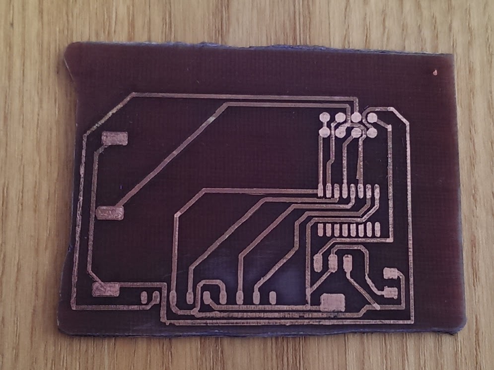
FeCl3 is quite proven for etching of the PCB.


